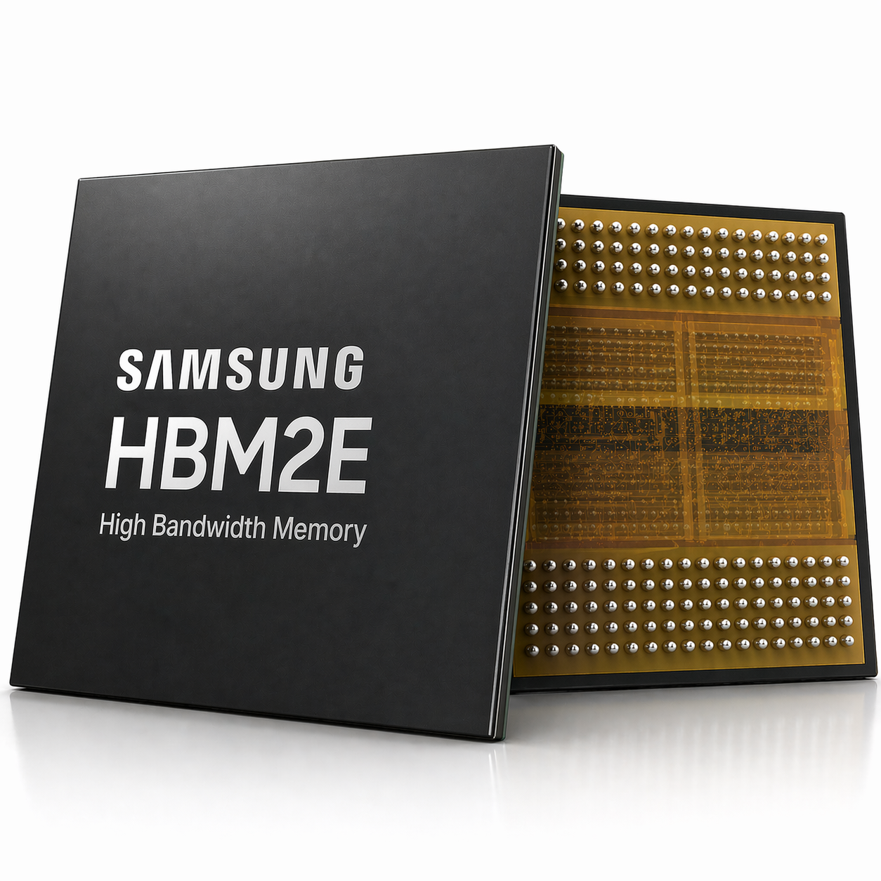
SamSung HBM2E Flashbolt - 8GB
SamSung HBM2E Flashbolt - 8GB
无法加载取货服务可用情况
SamSung HBM2E Flashbolt - 8GB
High Bandwidth Memory for AI and High Performance Computing
SamSung HBM2E Flashbolt 8GB is a high-bandwidth stacked DRAM solution developed for AI accelerators, data-center GPUs, and advanced high performance computing platforms. As an evolution of HBM2 technology, HBM2E increases per-stack bandwidth and memory density while maintaining signal integrity and thermal stability under sustained compute workloads.
Compared with earlier HBM2 generations such as Aquabolt, HBM2E Flashbolt improves pin speed and total stack throughput, enabling higher effective bandwidth for large-scale neural network training, simulation modeling, and parallel data processing.
Architecture and Bandwidth
- Memory Type: HBM2E
- Capacity: 8GB per stack
- I/O Width: 1024-bit
- Data Rate: Up to 3.6 Gbps per pin
- Bandwidth: Up to 460 GB/s per stack
- Technology: TSV (Through-Silicon Via) stacked DRAM
- Error Correction: On-Die ECC (ODECC)
With a 1024-bit wide interface and 3.6 Gbps signaling, a single HBM2E Flashbolt 8GB stack can deliver up to 460 GB/s bandwidth. In multi-stack accelerator configurations, aggregate bandwidth scales significantly, supporting high bandwidth memory for AI accelerators and deep learning processors.
Density and Compute Scaling
The 8GB capacity is achieved by stacking eight layers of 10nm-class 16Gb DRAM dies. Higher stack density reduces interconnect distance and improves bandwidth efficiency compared to traditional GDDR memory architectures.
For engineers designing Samsung HBM2E Flashbolt 8GB stack based systems, this configuration enables improved memory locality and sustained throughput for compute-intensive AI and HPC workloads.
Power Efficiency
HBM2E Flashbolt enhances power efficiency compared to earlier HBM2 implementations. Optimized internal routing and expanded power bump distribution improve voltage stability under high data burst conditions.
This makes it suitable for data center class GPU memory systems where thermal envelope and long-duration reliability are critical design constraints.
Reliability and Data Integrity
Integrated On-Die ECC allows internal error detection and correction before data transmission, improving stability in large-scale AI clusters and supercomputing deployments.
Part Number List
- KHAA44801B-MC17
- KHAA44801B-MC16
FAQ
Q1: What is the difference between HBM2 and HBM2E?
HBM2E increases per-pin data rate and stack density compared with HBM2. While both use a 1024-bit wide I/O interface, HBM2E delivers higher bandwidth and improved efficiency for AI and HPC systems.
Q2: Is HBM2E Flashbolt a memory module?
No. HBM2E Flashbolt is a TSV-based stacked DRAM package designed for integration onto an interposer or substrate within GPU and accelerator architectures.
Q3: What applications typically use HBM2E 8GB stacks?
AI training accelerators, deep learning processors, scientific computing systems, and high-end GPU platforms requiring high bandwidth memory.
Share