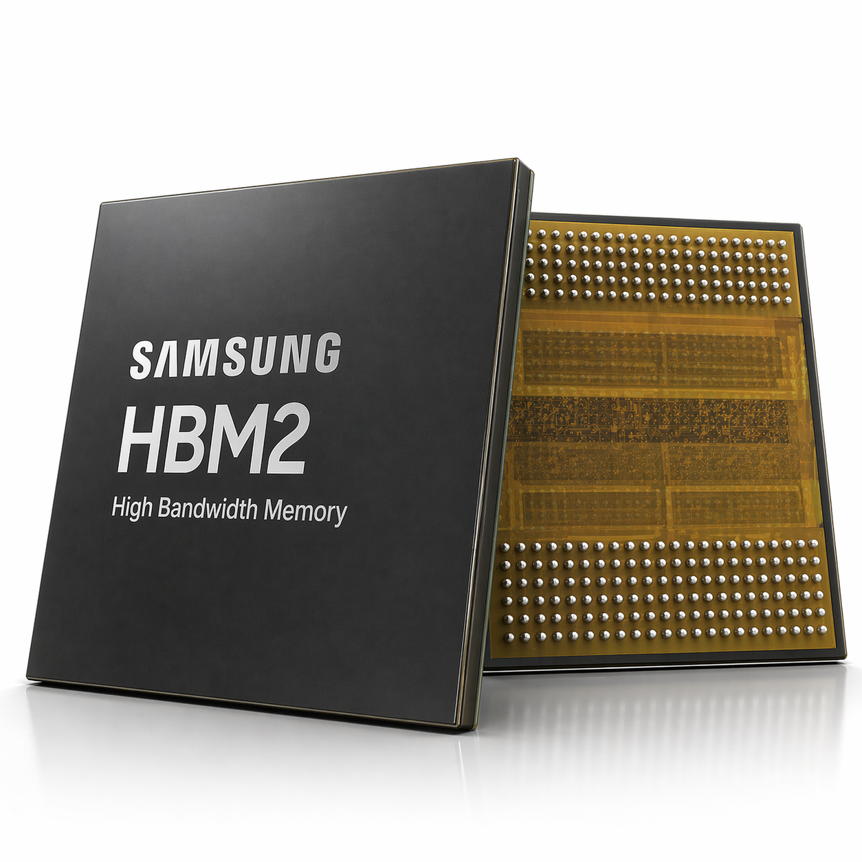
Samsung HBM2 Flarebolt - 4Gb / 8Gb
Samsung HBM2 Flarebolt - 4Gb / 8Gb
无法加载取货服务可用情况
Samsung HBM2 Flarebolt - 4Gb / 8Gb
High Bandwidth Memory for AI, HPC and Graphics Processing
Samsung HBM2 Flarebolt is a high-bandwidth DRAM solution built on TSV (Through-Silicon Via) stacking technology. Designed for AI accelerators, high performance computing systems, and advanced graphics processors, HBM2 Flarebolt delivers substantial bandwidth improvements while maintaining lower operating voltage and compact package integration.
Available in 4Gb and 8Gb die densities, Flarebolt enables scalable memory stack configurations suitable for data-intensive GPU and networking applications.
Technical Overview
- Memory Type: HBM2
- Die Density: 4Gb / 8Gb DRAM die
- Interface Width: 1024-bit
- Channels: 8 channels per stack
- Bandwidth: Up to 256 GB/s per stack
- System Bandwidth: Up to 1 TB/s (multi-stack configuration)
- Operating Voltage: 1.35 V
- Technology: TSV stacked architecture
With a 1024-bit interface and 8 independent channels, a single HBM2 Flarebolt stack can deliver up to 256 GB/s bandwidth. In multi-stack GPU configurations, aggregate system memory bandwidth can scale to approximately 1 TB/s, supporting high bandwidth memory for AI accelerators and advanced HPC environments.
Architecture and Performance Scaling
HBM2 Flarebolt increases I/O density to 1,024 data lines, enabling significantly higher throughput compared to GDDR5-based memory systems. The wide interface design reduces reliance on extremely high clock frequencies, improving signal integrity and thermal stability.
Compared to traditional GDDR5 memory architectures, HBM2 Flarebolt offers substantially higher bandwidth per watt and improved performance per unit PCB area.
Power Efficiency
Operating at 1.35 V, HBM2 Flarebolt reduces power consumption by approximately 20% compared to 1.5 V GDDR5 solutions. Lower voltage operation improves overall system efficiency in GPU clusters and high-density accelerator platforms.
Compact Integration
HBM2 integrates memory stacks directly adjacent to the processor using silicon interposer technology. This reduces PCB footprint by up to 94% compared to conventional GDDR-based designs, enabling higher compute density and improved signal routing efficiency.
Part Numbers
- KHA843801B-MC12
- KHA883901B-MC12
FAQ
Q1: Is Samsung HBM2 Flarebolt a DIMM or plug-in module?
No. HBM2 Flarebolt is a stacked DRAM component integrated onto a silicon interposer alongside GPU or accelerator dies. It is not a pluggable memory module.
Q2: What does 4Gb or 8Gb refer to?
4Gb and 8Gb indicate the per-die storage density. Multiple dies are vertically stacked to form a complete HBM2 memory stack.
Q3: What is the difference between HBM2 Flarebolt and HBM2E?
HBM2E increases die density and per-pin data rate compared to HBM2. While both use a 1024-bit interface, HBM2E supports higher total stack capacity and improved bandwidth efficiency.
Share