DDR3 2Gb SDRAM (F-die) – 1600 / 1866 / 2133 Mbps
DDR3 2Gb SDRAM (F-die) – 1600 / 1866 / 2133 Mbps
无法加载取货服务可用情况
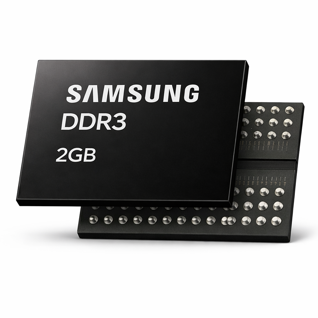
Samsung DDR3 2Gb SDRAM (F-die) – 1600 / 1866 / 2133 Mbps
2Gb DDR3 FBGA Memory for Legacy Platforms, Industrial Boards and System Maintenance
Samsung DDR3 2Gb F-die SDRAM is designed for stable, long-cycle system applications requiring consistent bandwidth and low operating power. Supporting transfer rates up to 2133Mb/sec per pin (DDR3-2133), this device remains widely deployed in embedded platforms, desktops, notebooks, automotive electronics and medical control systems built around DDR3 architecture.
For customers sourcing Samsung DDR3 2Gb 2133 memory chip, maintaining DDR3 1600 1866 industrial DRAM supply, or qualifying 2Gb DDR3 FBGA x8 device for legacy production, this series provides a practical solution without migrating to newer memory generations.
Architecture & Electrical Characteristics
- Density: 2Gb
- Die revision: F-die
- Organization: 32Mbit × 8 I/Os × 8 banks
- Speed grades: DDR3-1600 / DDR3-1866 / DDR3-2133
- Transfer rate: Up to 2133Mb/sec/pin
- Voltage: 1.5V ± 0.075V (VDD / VDDQ)
- Package: 78-ball FBGA (x8)
- Differential clock input (CK / CK#)
- DQS-based source synchronous data interface
- RAS/CAS multiplexed addressing
- Supported features: Posted CAS, Programmable CWL, Internal Self Calibration, On-Die Termination (ODT), Asynchronous Reset
Power & Performance Positioning
Compared with DDR2 platforms, DDR3 architecture doubles bandwidth while reducing power consumption by up to 30%. Built on Samsung 30nm class DRAM technology, this device supports efficient thermal behavior and lower total cost of ownership in power-sensitive systems.
Part Number List – Samsung DDR3 2Gb Series
| Part Number | Density | Package |
|---|---|---|
| K4B2G1646F-BYNB | 2Gb | FBGA |
| K4B2G0846F-BCK0 | 2Gb | FBGA |
| K4B2G0846F-BCMA | 2Gb | FBGA |
| K4B2G0846F-BCNB | 2Gb | FBGA |
| K4B2G0846F-BMK0 | 2Gb | FBGA |
| K4B2G0846F-BMMA | 2Gb | FBGA |
| K4B2G0846F-BYMA | 2Gb | FBGA |
| K4B2G0846F-BYNB | 2Gb | FBGA |
| K4B2G1646F-BCK0 | 2Gb | FBGA |
| K4B2G1646F-BCMA | 2Gb | FBGA |
| K4B2G1646F-BCNB | 2Gb | FBGA |
| K4B2G1646F-BFMA | 2Gb | FBGA |
| K4B2G1646F-BHMA | 2Gb | FBGA |
| K4B2G1646F-BMK0 | 2Gb | FBGA |
| K4B2G1646F-BMMA | 2Gb | FBGA |
FAQ – Technical Clarification
1. What system clock rates are supported?
This series supports DDR3-1600, DDR3-1866, and DDR3-2133 speed grades, delivering up to 2133Mb/sec per pin depending on controller configuration.
2. What are the voltage requirements for board design?
The device operates at a single 1.5V ±0.075V supply for both VDD and VDDQ, consistent with standard DDR3 system design.
3. What packaging and bus width configuration is used?
The 2Gb F-die device is organized as 32Mbit × 8 I/Os × 8 banks and supplied in a 78-ball FBGA (x8) package.
SOURCEMEMORYCHIPS
Your Leading Global Supplier for Professional Memory Chip Sourcing
WhatsApp: +1 702 886 6700
Email: sales@sourcememorychips.com
Fast response for DDR, NAND, eMMC, LPDDR and industrial memory inquiries.
Share